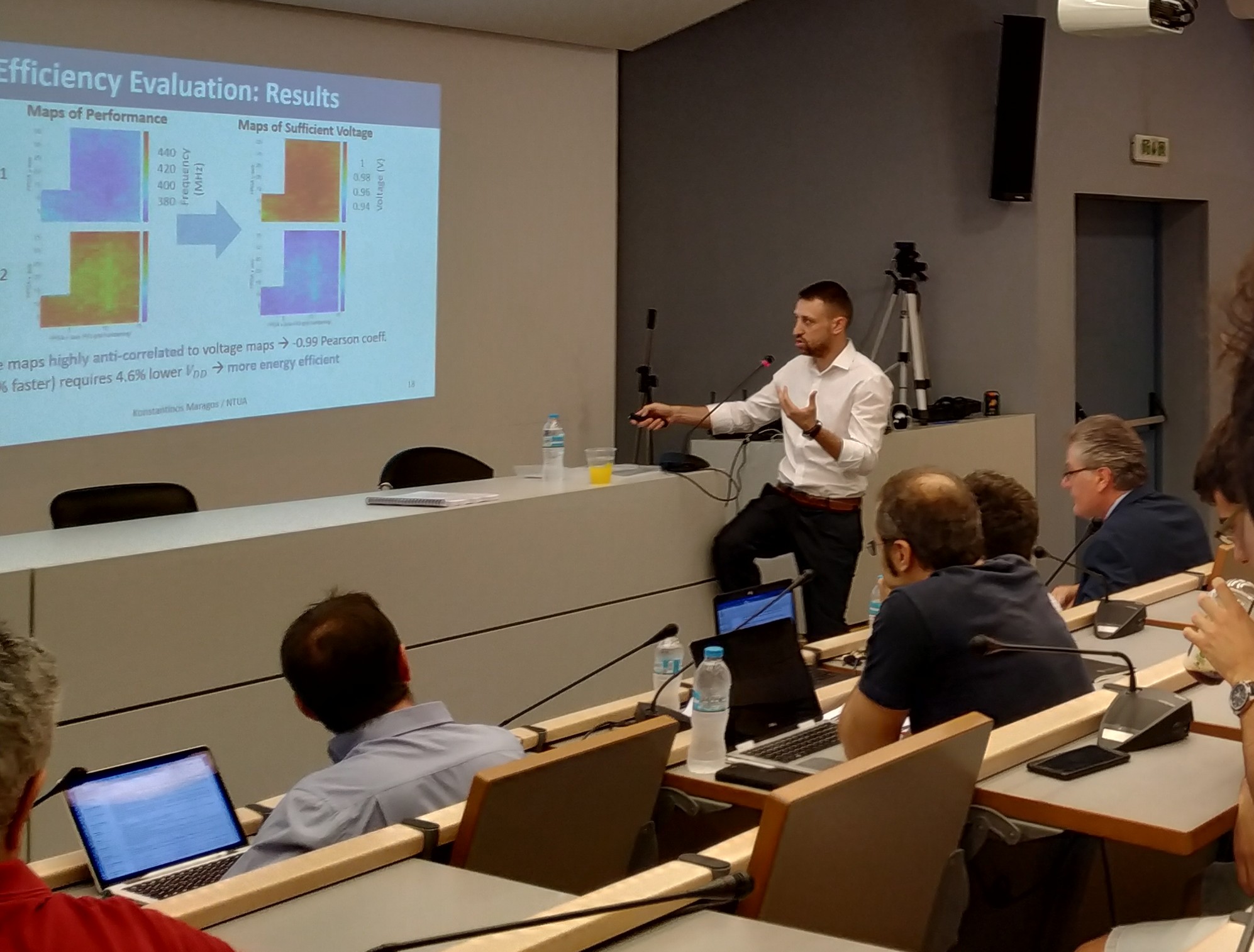
Konstantinos Maragos presented his PhD thesis entitled “Exploitation of Process Variability in FPGAs Devices”
Extended Abstract:
Transistor scaling is one of the major factors driving the continuous advancements in performance of semiconductor chips. However, as transistors’ size reach the atomic scale, the manufacturing process becomes increasingly challenging and inefficient from an economic standpoint. The industry struggles to keep up with Moore’s law, while the speed and power gains arise as we move from one technology node to the next are reduced compared to past trends. To alleviate this performance gap, alternative solutions have been proposed including heterogeneous computing, more efficient architectures, 3D technology, in-memory computing, etc. In this context, one of the contributions of the current research work, relies on the presentation of HW accelerators based on FPGA platforms for improved performance figures. We describe design methodologies for the development of efficient architectures based on sophisticated parallelization methods, design space explorations and a custom HW partitioning methodology for multi-FPGA systems. We demonstrate the benefits arise by the aforementioned methodologies on multiple application fields considering diverse FPGA platforms; conventional, SoC- and multi-FPGAs. Another challenge which becomes more significant with further technology scaling is the mitigation of major reliability issues, such as process variability, voltage drop effects and thermal dissipation. To cope with the aforementioned issues and provide acceptable solutions, the chip vendors impose global and conservative guard-bands in the operation of their manufactured chips. The guard-bands are defined according to the extreme-case process corners of the manufactured chips. Such pessimistic strategy, however, do not exploit the actual performance capabilities of the individual chips and do not adapt to those operating conditions (e.g., IR-drop) that strongly depend upon the individual characteristics of an application. Therefore, significant performance is lost, either in terms of frequency or power consumption. In the current research work, our core contribution is based on the delivery of adaptive solutions with respect to the quality of the underlying silicon and the specifics of the application running on the chip. We specifically target on the performance enhancement of present-day and future FPGA-based processing systems. We begin with the presentation of a methodology for the evaluation of process variability in commercial off-the-shelf FPGA devices. The proposed methodology is based on the generation of variability maps characterizing in a fine-grain resolution the performance variation across the FPGA fabric. Utilizing the proposed methodology, we provide variability results considering multiple and of diverse types (conventional, SoC) 28nm FPGA devices. We evaluate the impact of variability on larger realistic designs and establish the usage of variability maps as performance prediction tools. Motivated by the performance gains arise by the exploitation of process variability and operation guard-bands, we introduce a framework for the delivery of more efficient solutions in terms of frequency and/or voltage. The proposed framework bases on variability maps for the mapping of a given design to the most efficient region (intra-die) and device (inter-die), as well as frequency and voltage scaling methods to tune the FPGA operation with respect to user requirements. The main advantages of the proposed framework compared to prior art, are the exploitation of process variability for improved performance gains and its application at user level, without requiring the modification of CAD’s tool or design netlist. Depending on the underlying device(s) and the given application, the proposed framework is able to deliver even 2x better performance compared to that of STA estimations.


